
A New Step for Conductive Copper Filament: Why Kupros Cu29 Is Bringing Embedded Electronics with FDM Back into Focus
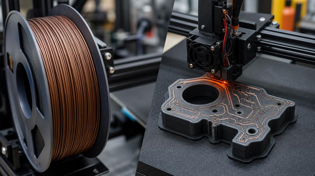
According to 3Dnatives’ August 6, 2026 report, Kupros is positioning its conductive copper-based filament called Cu29 for embedded electronics manufacturing with FDM. The critical point here is that the material is presented as being processable on standard FDM machines. In other words, this is not just a new material announcement; it points to a step that brings the idea of sensors, conductive traces, and geometry-embedded electronics a little closer to the desktop and industrial FDM world.
As clearly stated in the report, Cu29 is not simply solid copper wire wound onto a spool. Kupros describes it as a family of conductive filaments that use copper as part of the formulation. The goal is to produce conductive lines that follow the shape of the part, embedded sensors, signal-carrying channels, and some antenna-like structures, without forcing conductive paths onto a flat circuit board. Especially in complex-shaped FDM parts, this approach stands out because it allows the mechanical body and electrical function to come together in the same prototype.
Why does it matter?
For Ucuz3D readers, the value of this news lies in how it connects the concept of electronic parts more closely to FDM part design. Today, in many projects, the plastic body is developed separately, while wiring and connection solutions are handled separately. If conductive paths can truly be integrated into the print geometry more naturally, the design cycle could become shorter for custom enclosures, test fixtures, sensor carriers, robotic subassemblies, and low-volume R&D parts. This is exactly why a professional 3d printing service approach still remains critical, especially for teams that want to validate the body first and then move on to functional revisions.
Another strong signal in the report is that Kupros reportedly received pre-order interest from institutions such as NASA, Northrop, and Boeing before the material was fully ready. This alone does not mean technical validation; however, it does show that the market feels a real need for this kind of FDM material. The 3Dnatives report also explains that early demand has been concentrated particularly on the aerospace R&D side, driven by expectations such as fewer wire harnesses, fewer connection points, and faster electro-mechanical design iteration.
What is the practical meaning for FDM users?
In the short term, this development does not mean that everyone will start producing fully functional electronics directly on their desktop printer. For a conductive filament to be truly useful in real-life applications, printing alone is not enough; contact reliability, insulation strategy, trace width, resistance behavior, thermal load, and long-term durability also matter. Still, the direction in prototyping is clear: combining mechanical and electrical function in the same FDM part is now being discussed more seriously. This could create new hybrid part scenarios in the future, especially for teams working with engineering materials.
Another important detail is that Cu29 is positioned to work on standard FDM hardware. If this approach proves practical in real-world use, the gap between much more expensive specialized electronics manufacturing equipment and traditional filament-based production could narrow. For designers, this means the ability to plan both the structural body and certain conductive routes within a single part. On the cost side, however, decisions should be based not only on the new material itself, but also on part size, number of revisions, and production volume; that is why it is healthier to evaluate the logic of price per gram together with the overall part economics.
Why is caution necessary?
Some of the performance claims mentioned in the report come from the company itself. For this reason, it would not be right to draw firm conclusions before independent validation, application examples, and field reliability are seen. In addition, using conductive filament may require process control that differs from standard PLA or PETG printing logic. Nozzle wear, surface contact quality, print orientation, and any post-print connections can directly affect real performance. Even so, the main message of the report is clear: FDM is moving beyond being just a shape-making manufacturing method and is approaching a new threshold in the field of functional parts.
In short, the Kupros Cu29 news shows that material innovation is still one of the most exciting areas in the FDM world. For today, the most realistic use cases will probably be advanced prototyping, test parts, and low-volume special-purpose applications. Once your file is ready, the most sensible path is still to validate mechanical prototypes quickly through an online 3d printing workflow, and then develop the design step by step for more advanced stages such as electronic integration.



 Türkçe
 العربية
 Русский
 فارسی
فارسی Deutsch